Application Lab Services
Product Development. Customer Training. Continuous Improvement.
CVDE develops advanced materials, technologies, and process solutions. We qualify CVDE equipment and technology capabilities and validate new hardware and recipes.
Process Solutions and Performance
Our process engineers and our Application Laboratory test center facilitate product development for our customers with feasibility trials to demonstrate process systems, validate equipment performance for specific process requirements, and optimize and improve equipment performance.
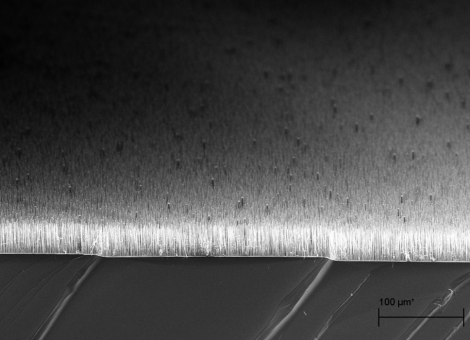
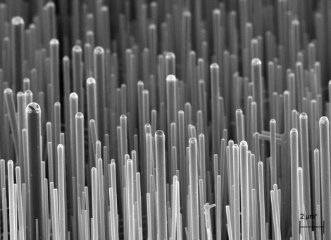
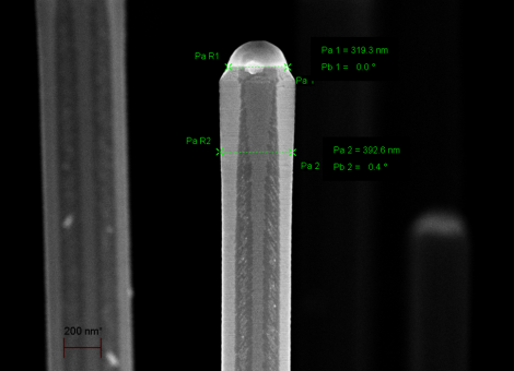
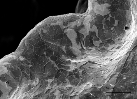
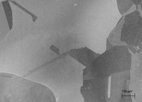
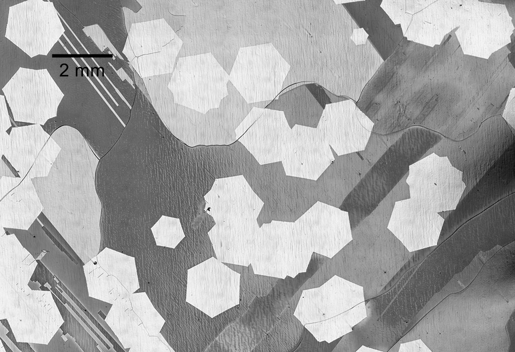
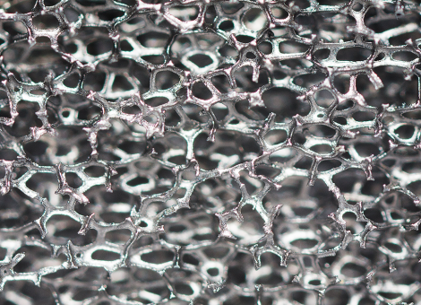
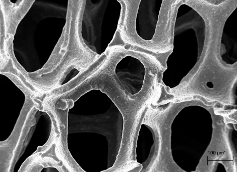
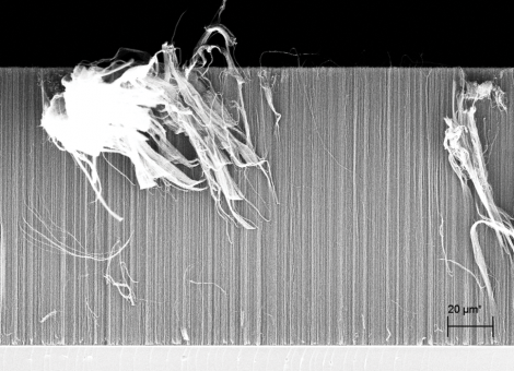
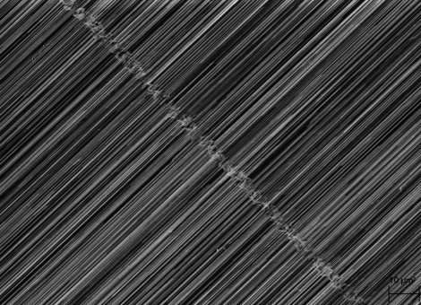
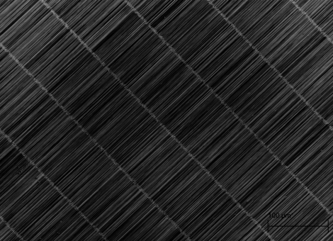
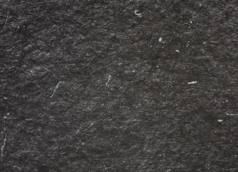
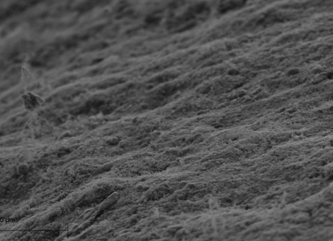
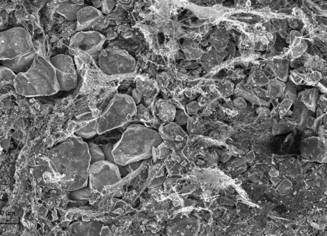
Our process engineers have the expertise, along with our simulation and modeling in our Application Laboratory to develop and innovate advanced materials including carbon nanotubes (CNTs) and processes including powder coating. Defining the path from laboratory scale to mass production with advanced solutions in state-of-the-art chemical vapor deposition and thermal process equipment is a primary focus.
Whether you are trying to develop a new thin film deposition process solution or looking to transfer your intellectual property to a pilot line or to the full production stage, CVD Equipment Corporation can provide cost-efficient solutions.
For Application Lab services or material samples, please fill in the following information
* These fields are required.
Application Lab Capabilities:
Customer training center where we can provide demonstrations of our CVD systems for thin film deposition and nanomaterial growth processes
Bays prepared and ready to install your equipment with live reactant gas supply and exhaust treatment for factory process demonstrations and initial process development prior to taking delivery of your equipment
Prototype process demonstration capabilities to provide you with samples in support of capital equipment procurement
Accelerated lifetime testing of our equipment subcomponent designs including heaters, vacuum and exhaust systems, gas delivery and gas injection systems, plasma systems, and automation systems
Testing and benchmarking of custom designs to verify that components and software meet your R&D and production needs
About Us
Over 40 years of expertise in CVD and thermal process equipment design and manufacturing.
“enabling tomorrow’s technologies ™ ”